Callouts: Main board ANOVA_PRO_MAIN_V2.0 - component side
Source: FCC ID 2APBOAN600, internal-photos exhibit 3999178 (2018 sample), page 2, lower photo (779x536)
Annotated image: images/annotated/main_component-side.png
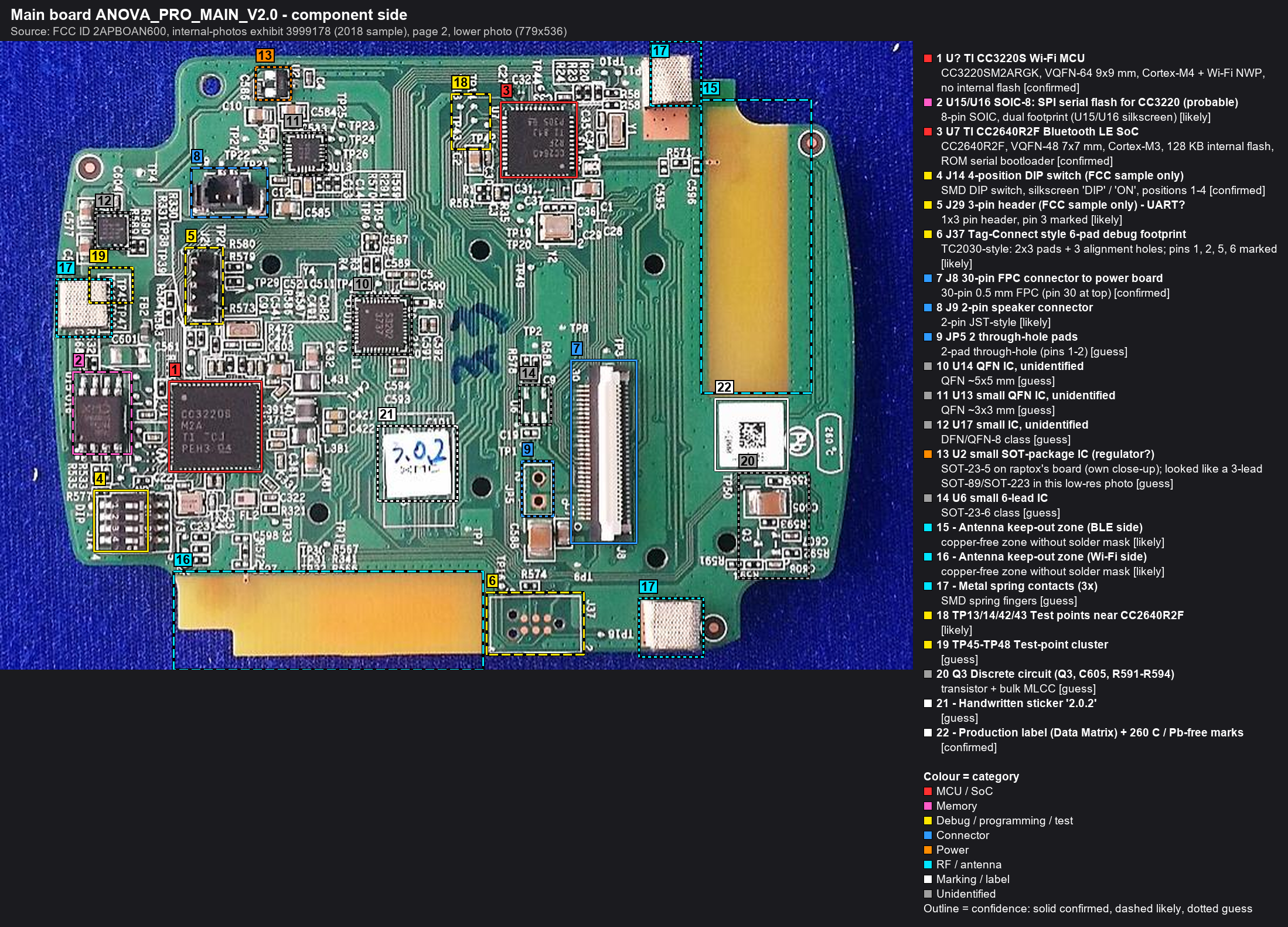
| # | Ref | Identification | Part / marking | Category | Confidence | Notes |
|---|---|---|---|---|---|---|
| 1 | U? | TI CC3220S Wi-Fi MCU | CC3220SM2ARGK, VQFN-64 9x9 mm, Cortex-M4 + Wi-Fi NWP, no internal flash marking: CC3220S M2A / TI ?CJ / PEH3 G4 |
MCU / SoC | confirmed | Main Wi-Fi SoC. The S (non-F) variant boots its application image from external SPI serial flash into RAM, so firmware lives in the SOIC-8 next to it. Refdes is hidden under the chip label area. |
| 2 | U15/U16 | SOIC-8: SPI serial flash for CC3220 (probable) | 8-pin SOIC, dual footprint (U15/U16 silkscreen) marking: illegible at FCC resolution |
Memory | likely | Only 8-pin package next to the CC3220S, which needs an external SPI flash. Primary recovery target: read with a SOIC clip only when the board is unpowered or with the CC3220 held in reset. Read the marking on the real board. |
| 3 | U7 | TI CC2640R2F Bluetooth LE SoC | CC2640R2F, VQFN-48 7x7 mm, Cortex-M3, 128 KB internal flash, ROM serial bootloader marking: CC2640 / R2F / TI 813 / P305 G4 (printed upside down in photo) |
MCU / SoC | confirmed | Second MCU with its own firmware (FCC BLE report: Bluetooth LE 4.2). Debug via cJTAG/JTAG. Which MCU drives display/keys and talks to the power board is still unknown. |
| 4 | J14 | 4-position DIP switch (FCC sample only) | SMD DIP switch, silkscreen 'DIP' / 'ON', positions 1-4 | Debug / programming / test | confirmed | Not fitted on raptox's production unit (empty footprint). Hypothesis: CC3220 SOP boot-mode straps. Next to R533/R535/R577. |
| 5 | J29 | 3-pin header (FCC sample only) - UART? | 1x3 pin header, pin 3 marked | Debug / programming / test | likely | Fitted on the FCC sample, empty holes on raptox's unit (pin count confirmed from raptox's photos). Near R573/R579/R580 and TP28/TP29. Candidate CC3220 UART (TX/RX/GND). |
| 6 | J37 | Tag-Connect style 6-pad debug footprint | TC2030-style: 2x3 pads + 3 alignment holes; pins 1, 2, 5, 6 marked | Debug / programming / test | likely | Sits back-to-back with J38 on the LED side. Typical TI usage: JTAG/SWD or cJTAG (TMS, TCK, RESET, VDD, GND). Likely one footprint per MCU (CC3220S / CC2640R2F). Verify by continuity. |
| 7 | J8 | 30-pin FPC connector to power board | 30-pin 0.5 mm FPC (pin 30 at top) | Connector | confirmed | White ribbon to J8 on the power board (see assembly photo). Carries supply rails and control/sense signals; the pinout is TODO. |
| 8 | J9 | 2-pin speaker connector | 2-pin JST-style | Connector | likely | Yellow/black pair into the housing (assembly photo). A community repair report mentions 'speaker wires' on the display board, so this is probably the beeper/speaker. |
| 9 | JP5 | 2 through-hole pads | 2-pad through-hole (pins 1-2) | Connector | guess | Next to C588. Wire solder point or jumper. Function unknown. |
| 10 | U14 | QFN IC, unidentified | QFN ~5x5 mm marking: '3737' legible, first line unreadable in the FCC photo |
Unidentified | guess | Same position and '3737' as U14 on raptox's board, which reads T3018 / 3737: probably the same part. Candidates: LED matrix driver (about 135 discrete LEDs on the other side) or capacitive-touch controller. |
| 11 | U13 | small QFN IC, unidentified | QFN ~3x3 mm marking: illegible |
Unidentified | guess | Surrounded by TP21-TP26 (good probing points). Near U2 and J9. |
| 12 | U17 | small IC, unidentified | DFN/QFN-8 class marking: illegible |
Unidentified | guess | Next to R589/R590. Could be an I2C sensor, EEPROM or level shifter. |
| 13 | U2 | small SOT-package IC (regulator?) | SOT-23-5 on raptox's board (own close-up); looked like a 3-lead SOT-89/SOT-223 in this low-res photo | Power | guess | Probably a linear regulator generating a logic rail. Measure input/output on the real board. |
| 14 | U6 | small 6-lead IC | SOT-23-6 class | Unidentified | guess | Next to the FPC connector J8. Possibly ESD protection, a level shifter or a load switch on the power-board interface. |
| 15 | Antenna keep-out zone (BLE side) | copper-free zone without solder mask | RF / antenna | likely | Nearest antenna zone to CC2640R2F (U7). FCC reports list PCB antennas: BLE 2.21 dBi, Wi-Fi 2.45 dBi. | |
| 16 | Antenna keep-out zone (Wi-Fi side) | copper-free zone without solder mask | RF / antenna | likely | Nearest antenna zone to CC3220S. | |
| 17 | Metal spring contacts (3x) | SMD spring fingers | RF / antenna | guess | Probably ground/shield contacts to the housing or bezel. Possibly antenna-related. | |
| 18 | TP13/14/42/43 | Test points near CC2640R2F | Debug / programming / test | likely | Test-point cluster with traces running toward U7. Candidates: BLE debug or UART. Probe these on the real board. | |
| 19 | TP45-TP48 | Test-point cluster | Debug / programming / test | guess | Next to the left spring contact and U17. | |
| 20 | Q3 | Discrete circuit (Q3, C605, R591-R594) | transistor + bulk MLCC | Unidentified | guess | Function unknown. Candidates: buzzer driver, reset/power-good or supervisor. |
| 21 | Handwritten sticker '2.0.2' | marking: 2.0.2 (blue pen) over a printed label |
Marking / label | guess | Probably the firmware or hardware version of the FCC sample (2018). Also blue pen marks '33/35' nearby. | |
| 22 | Production label (Data Matrix) + 260 C / Pb-free marks | Marking / label | confirmed | PCB serial/lot label. Compare with raptox's unit to detect revision changes. |