Photo log
Original photos of raptox's unit (AN600-20 EU). They are stored byte-identical under images/own/<date>/ and never edited.
Derived crops and annotations are generated through annotations/crops.json and tools/.
Phone: 4080x3072 JPEG. Some files carry an EXIF rotation flag, which the tools apply.
2026-11-01: head opened, main board component side
| File | Shows | Used in |
|---|---|---|
01_head_front-glass-removed.jpg (camera IMG_20261101_135337_092.jpg) |
Head with the front glass removed, adhesive residue on the bezel | front_glass-off_own, disassembly |
02_bezel-and-main-board_hinged-out_side.jpg (camera IMG_20261101_135701_097.jpg) |
Bezel + main board hinged out, side view | - |
03_head-open_ffc-speaker-power-board.jpg (camera IMG_20261101_135707_251.jpg) |
Bezel lifted: FFC, speaker wires, speaker 20 / 219, power board in the tube |
head_open_own, disassembly |
04_main-board_component-side_angled.jpg (camera IMG_20261101_135712_858.jpg) |
Main board component side at an angle, FFC still connected | - |
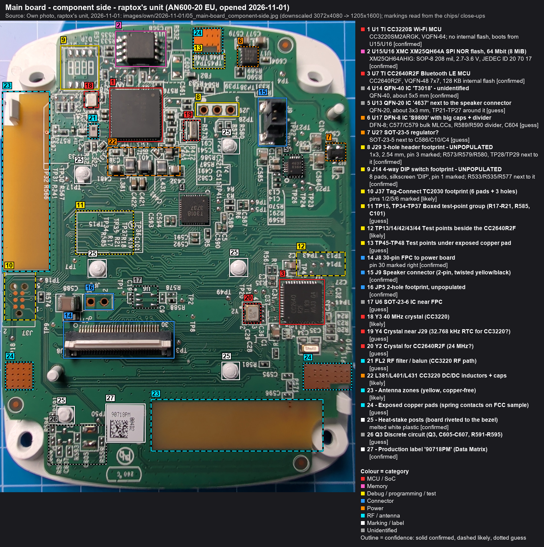
05_main-board_component-side.jpg (camera IMG_20261101_140052_627.jpg) |
Main board component side, straight on (reference photo) | main_component-side_own → annotated |


Chip close-ups (chips/)
| File | Shows | Crop |
|---|---|---|
01_U1-cc3220s_U15-flash_Y3_J14.jpg (camera IMG_20261101_140511_295.jpg) |
U15/U16 XMC QH64AHIG, U1 CC3220S M2A, Y3, J14 DIP footprint | chip_U1-U15_cc3220-flash |
02_U14-t3018.jpg (camera IMG_20261101_140519_507.jpg) |
U14 T3018 / 3737 |
chip_U14_t3018 |
03_U7-cc2640r2f.jpg (camera IMG_20261101_140524_443.jpg) |
U7 CC2640R2F, TP13/14/42/43/44 | chip_U7_cc2640r2f |
04_U17-dfn8_J9_J29-corner.jpg (camera IMG_20261101_140530_191.jpg) |
U17 DFN-8, J9, J29 corner | chip_U17 |
05_U13-4637_TP21-27_J9_U2.jpg (camera IMG_20261101_140534_792.jpg) |
U13 4637 / 638A, TP21-27, J9, U2 |
chip_U13_J9 |
06_J29-footprint_TP28-29_Y4.jpg (camera IMG_20261101_140543_109.jpg) |
J29 3-hole footprint, TP28/TP29, Y4 | chip_J29 |


Next: microscope survey (first job when the Andonstar AD409 Pro-ES arrives)
Goal: one stitched, measurable mosaic per board side to replace the phone photo as the reference, plus sharp close-ups of every marking and debug footprint.
Sets, in order
- Main board, component side (raptox's unit): full mosaic.
- Close-ups at higher magnification, not stitched:
- markings that are partly illegible now: U17, U2, U13, U14
- J14 pads, J29, J37/J38 straight on, TP groups
- laser-etched markings: take each one twice, with diffuse light and with light from the side
- layer-count evidence, all non-destructive:
- the board edge at the break-off tab marks: look for copper lines in the cross-section
- the RF traces from U1 and U7 to their antennas (width and gap to ground, with the ruler frame)
- any fab or layer markings
- backlight with the Elgato Key Light:
- Setup:
- unplug the FFC at J8 and the speaker at J9
- lay the bezel + board assembly bezel-down on the panel. The board is heat-staked to the bezel, but the white light guide passes light (the segment walls will cast shadows).
- Key Light at full brightness, microscope lights off, room dark, exposure locked
- Method: shoot each spot twice without moving the board, with top light and with backlight. Copper on any layer shows as a shadow. A spot that is dark in backlight but has no copper on the component side, nor in the FCC LED-side photo, has inner copper.
- It is transillumination, not X-ray: chips and other parts block the light.
- Power board, both sides, if it can be removed (unplugged, see the mains rule). Its ICs (U2, U10, ...) are unknown, and one may be an MCU.
- Main board LED side: only if the board ever comes off the bezel. Not needed now.
Capture protocol (mosaic sets)
- Board:
- unpowered, flat on a matte background, wrist strap on
- move the board, not the microscope
- slide it along a straightedge so the rotation stays constant
- Grid: about 40 % overlap in both directions, row by row in a serpentine order.
- Settings:
- one magnification and one focus setting for the whole set. Refocusing also shifts and rescales the image (Elektor review), so it breaks the stitch.
- lock exposure and white balance if the menu allows it, and keep the same light for every tile
- Scale: first frame of each set = a mm ruler lying in the board plane, at the same settings. It gives mm/px for the whole set.
- Resolution: the menu goes up to 5600 x 4200 ("24M"), but the sensor is 4 MP, so that is interpolated (likely, per the manual's specs). On arrival, shoot one frame at each setting and compare the detail. Use the smallest setting that loses nothing.
- Saving settings: the device only keeps its settings if you switch it off with a long press on the power button. Pulling the power loses them (manual, FAQ 3).
- Depth of field and parallax: choose a magnification where the chips and pads are sharp. Tall parts (caps, connectors, inductors) will blur and lean between tiles because the lens is not telecentric. That is expected, and the close-ups cover them.
- What the PC can control (source: AD409 Pro user manual Ver 01, https://electrokit.com/upload/quick/1a/a6/873e_AD409-pro_users_manual-Ver_01_1.pdf; the Pro-ES is the same unit plus the endoscope, likely):
- Manual only:
- magnification = height of the monitor on the column
- focus = the knob
- the two base lights
- Zoom+/- buttons: digital zoom only. Leave them at 1x for mosaics.
- USB "PC Camera" mode:
- select it on the microscope after plugging in the data cable (not the power cable)
- Windows lists it as a USB video device named "USB Camera", so it is a standard webcam (UVC: likely). Python/OpenCV can grab frames without Andonstar's "Microscope Measure" software.
- Maximum USB resolution and which camera controls (exposure, WB) are exposed: unknown, check on arrival.
- Wi-Fi (the manual calls it a test function):
- needs a microSD card inserted; app "Ucam Dashcam"; access point
Andonstar-…, default password 12345678 - a dashcam app suggests a dashcam SoC. If it is a Novatek one, there is a known HTTP API (
cmd=1001= take a photo, plus file listing and download): guess. - Probe it only with read-only requests. Never send format, delete or settings commands.
- needs a microSD card inserted; app "Ucam Dashcam"; access point
- IR remote: the microscope has an IR receiver. A Pico with an IR LED (and an IR receiver module to learn the codes) can press "capture" from the PC. This is the fallback for triggering full-resolution shots to the SD card.
- Ways to shoot:
- A: raptox shoots to the microSD card.
- B: capture assistant. It watches the USB live view and raptox slides the board. When the overlap is about 40 % and the image is still and sharp, it either saves the frame or triggers a full-resolution SD shot (over Wi-Fi or IR). It also keeps a coverage map, so no gaps. The SD files are imported byte-identical afterwards.
Storage and stitching (originals never edited, blobs never committed)
- Tiles are originals:
- copy them byte-identical to
images/own/<date>/micro/<set>/and verify the SHA-256 - log one row per set here: board/side, grid size, magnification, light, mm/px
- The mosaic is generated: a planned
tools/stitch/readsannotations/mosaics.json(set dir, grid order, scale) and writesimages/mosaics/<set>.jpg, which is never hand-edited. - The model is translation only (flat board, camera moved in X/Y), not a panorama warp.
- Board crops and annotations then come from it through
crops.jsonas usual. - Check every mosaic against known sizes: U1 body 9 mm, J14 pitch 1.27 mm. Also look at the seams that cross chips.
- Open point: a set can be hundreds of MB. Before the first commit, decide between Git LFS for
images/own/*/micro/and keeping the tiles out of git (with a copy off the machine).