Power board: ANOVA_PRO_POWER_REV01
Source: FCC 2APBOAN600 internal photos (2018 sample). Callout tables: top · bottom.
Mains voltage. The AC/DC module primary, fuse, relay, mains tabs and their solder joints on the bottom side are at line potential. Only work on this board unplugged, and discharge the bulk capacitor before touching it.
Top side
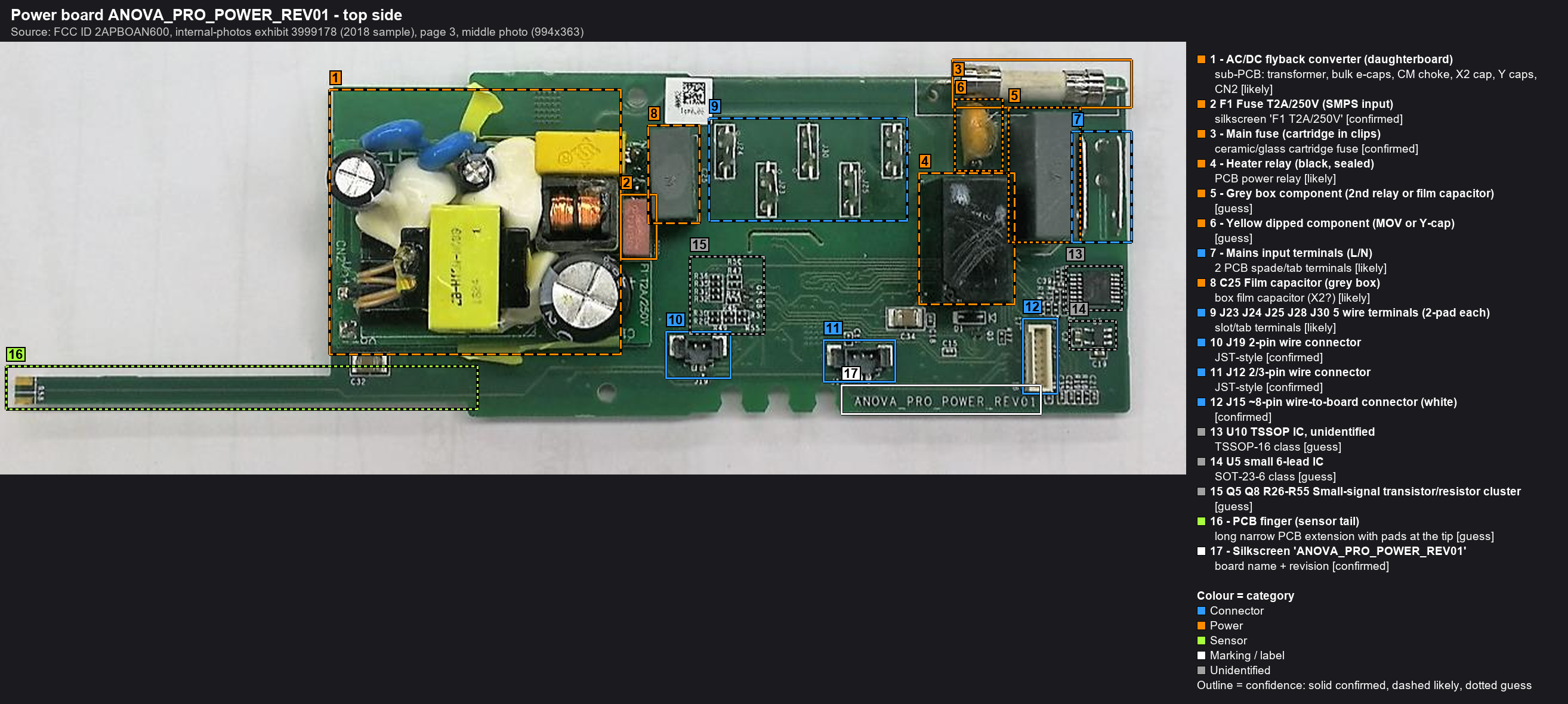
Source: FCC ID 2APBOAN600, internal-photos exhibit 3999178 (2018 sample).
| # | Item | Notes |
|---|---|---|
| 1 | AC/DC flyback daughterboard | Transformer, bulk e-caps, CM choke, X2/Y caps, CN2. Output voltage unknown (12 V or 5 V are typical). |
| 2 | F1 T2A/250V | Input fuse of the AC/DC module. Check continuity on the dead unit (unplugged). |
| 3 | Main cartridge fuse | Heater path. Rating not legible. |
| 4 | Black sealed relay | Heater switching (likely) |
| 5 | Grey box | Second relay or film cap (guess) |
| 6 | Yellow dipped part | MOV or Y-cap (guess) |
| 7 | Mains tabs (L/N) | |
| 8 | C25 film cap | |
| 9 | J23/J24/J25/J28/J30 | Five 2-pad wire terminals: heater, pump, thermal cut-off, ... (TBD) |
| 10-12 | J19 (2p), J12 (2-3p), J15 (about 8p) | Sensor/motor wiring (TBD) |
| 13-15 | U10 (TSSOP-16), U5 (SOT-23-6), Q5/Q8 cluster | Unidentified. Drivers and sensing (guess). |
| 16 | PCB finger | Reaches into the tube. Probably carries the temperature sensor at its tip. |
Bottom side (flipped top-to-bottom relative to the top photo)
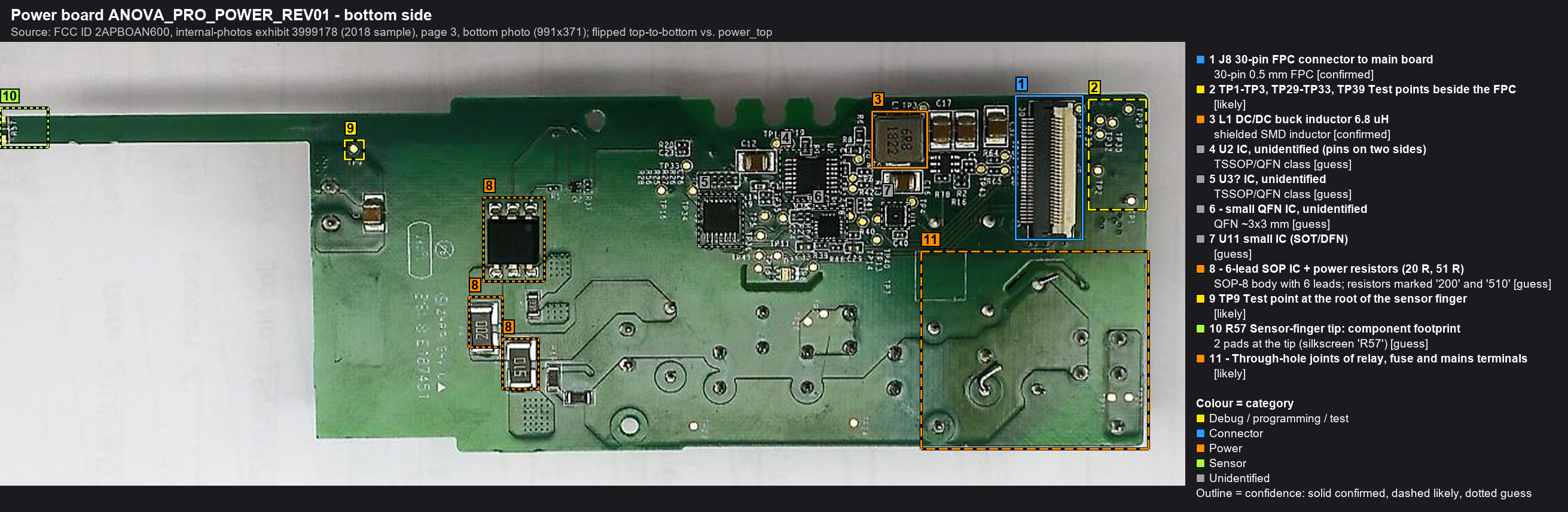
Source: FCC ID 2APBOAN600, internal-photos exhibit 3999178 (2018 sample).
| # | Item | Notes |
|---|---|---|
| 1 | J8 30-pin FPC | To main board J8. The logic supply is measured on the main-board side of this ribbon (bench-setup step 1a), never on this board while plugged in. |
| 2 | TP1-3, TP29-33, TP39 | Test points next to the FPC |
| 3 | L1 6R8 (6.8 uH) + C17/C31 | DC/DC buck, probably the logic rail |
| 4 | U2 | Biggest IC here, marking illegible. If this is an MCU, it has firmware too. |
| 5-7 | U3?, small QFN, U11 | Unidentified |
| 8 | 6-lead SOP + 20 R / 51 R power resistors | High-voltage part (offline regulator / driver?) under the AC/DC area |
| 9 | TP9 | Root of the sensor finger |
| 10 | R57 at the finger tip | Temperature-sensor position (guess) |
| 11 | Relay/fuse/mains solder joints | Mains |
Open questions
- AC/DC output voltage, and does it come up on the dead unit? (Measured at main-board J8 per bench-setup step 1a; nothing on this board is probed while plugged in.)
- Identify U2: MCU or not? Is there a debug or programming footprint on this board?
- What is the temperature sensor (NTC, RTD, digital)? Where is the pump driver?
- Wire-terminal assignment (J23-J30, J12, J15, J19).
- J8 FFC pinout (main to power).