Hardware overview
Status: main board confirmed on raptox's unit (2026-11-01); power board still from FCC photos (2018 sample, POWER_REV01). Confidence labels follow components.md. Nothing has been measured electrically yet.
Mechanical layout
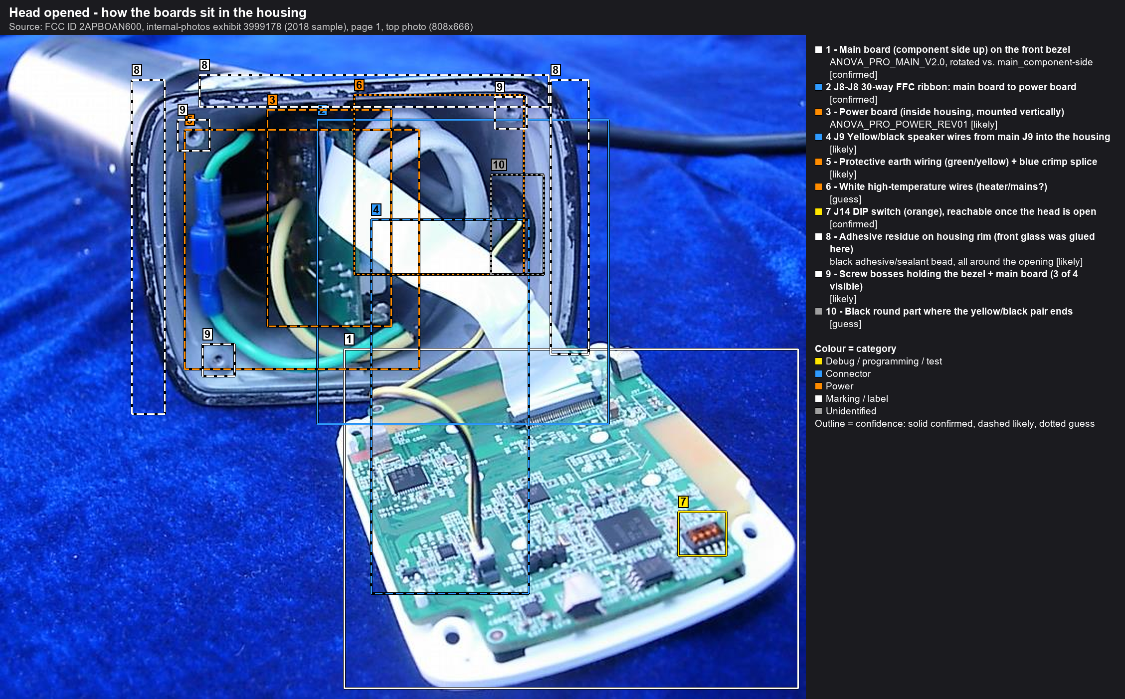
- The head holds the main board on the back of the front bezel, facing the user through a light guide and a black glass cover. See assembly.
- The power board stands vertically inside the head/tube. Its long PCB finger reaches down into the stainless tube, probably carrying the water-temperature sensor.
- A 30-way white FFC ribbon connects main board J8 to power board J8.
- Other wiring in the head:
- a yellow/black pair from main J9 into the housing
- protective earth (green/yellow, blue crimp splice)
- white high-temperature wires (heater/mains, probable)
Block diagram (provisional)
flowchart LR
  subgraph PWR["Power board ANOVA_PRO_POWER_REV01"]
    AC["AC mains in<br/>L/N tabs + main fuse"] --> SMPS["AC/DC flyback module<br/>F1 T2A/250V"]
    AC --> RLY["Heater relay"]
    RLY --> HEAT["Heater element<br/>(1200 W at 120 V, FCC sample;<br/>EU rating not yet read)"]
    SMPS --> BUCK["DC/DC buck<br/>L1 6.8 uH"]
    ICS["Unidentified ICs<br/>U2, U3?, U10, U11, U5<br/>(MCU? AFE? drivers?)"]
    TEMP["Sensor finger<br/>R57 at tip (NTC?)"] --> ICS
    ICS --> RLY
    PUMP["Pump motor<br/>(wire terminals)"]
    ICS --> PUMP
  end
  subgraph MAIN["Main board ANOVA_PRO_MAIN_V2.0"]
    WIFI["U1 TI CC3220S<br/>Wi-Fi MCU"] --- FLASH["U15/U16 XMC XM25QH64A<br/>8 MiB SPI NOR"]
    BLE["TI CC2640R2F<br/>BLE MCU"]
    UI["About 135 LEDs (3x4 digits)<br/>6 touch keys, U18 sensor"]
    U14["U14 T3018 QFN-40<br/>(LED / touch driver?)"] --- UI
    U13["U13 4637 QFN-20<br/>(audio?)"] --- SPK["Speaker (J9)"]
    DBG["Debug: J29 (1x3), J37/J38,<br/>J14 DIP pads, TPs"]
  end
  PWR == "30-way FFC J8 to J8" ==> MAIN
  WIFI -. "UART/SPI? (TBD)" .- BLE
Which MCU runs the UI and the cooking control loop, and how the CC3220S and CC2640R2F talk to each other, is unknown. These are the main questions for Phase 1/2.
Radios (from FCC test reports)
| Radio | Chip | Standard | Antenna | Conducted power |
|---|---|---|---|---|
| Wi-Fi 2.4 GHz | CC3220S | 802.11b/g/n HT20, ch 1-11 | PCB antenna, 2.45 dBi | 32.4 mW (grant) |
| Bluetooth LE | CC2640R2F | BLE 4.2, 1 Mbps GFSK | PCB antenna, 2.21 dBi | 3.5 mW (grant) |
The FCC sample was AN600-10, rated AC 120 V / 60 Hz, 1200 W. Samples were received 2018-08-01.
Boards
| Board | Photos | Doc |
|---|---|---|
Main ANOVA_PRO_MAIN_V2.0 |
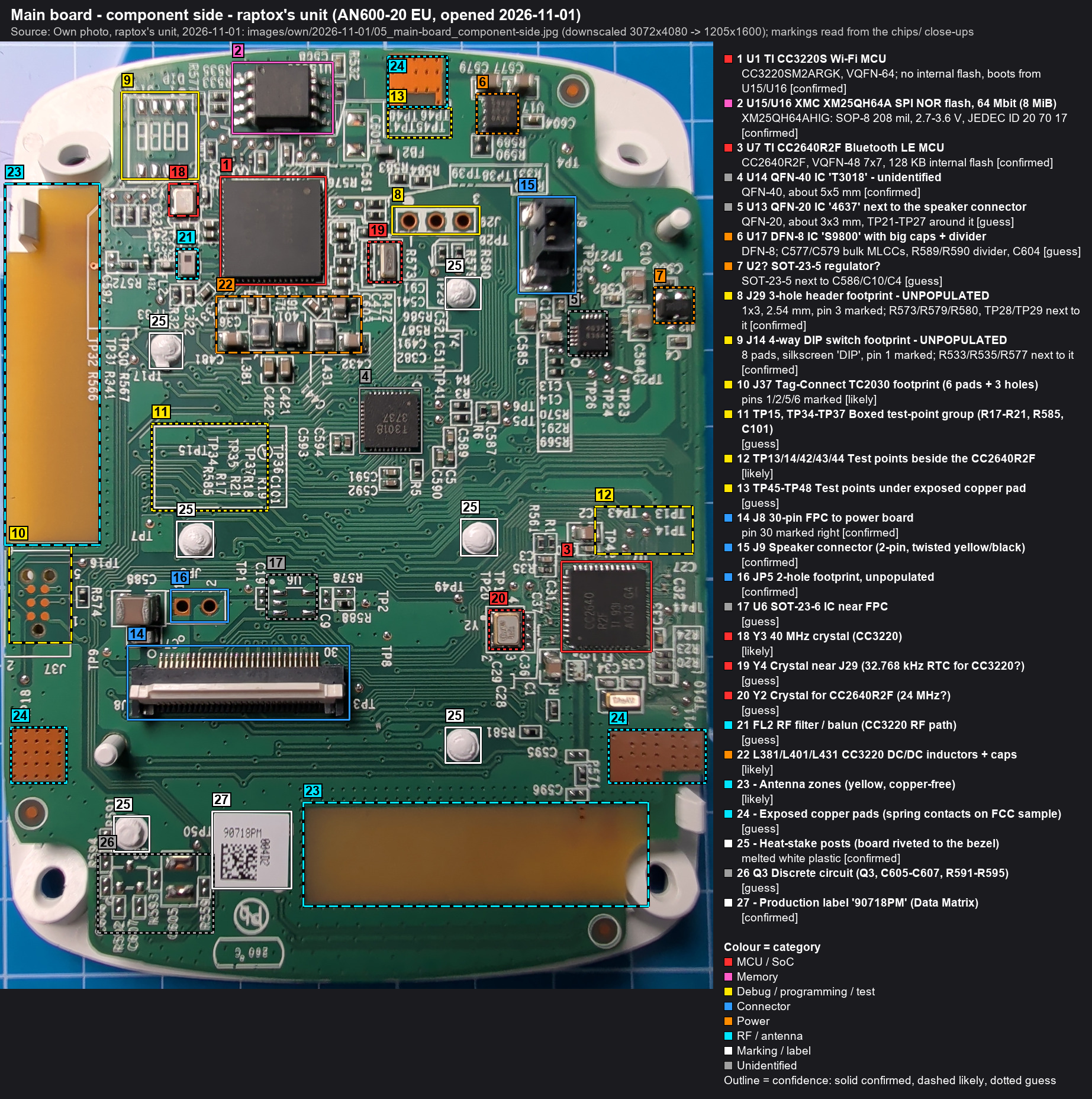
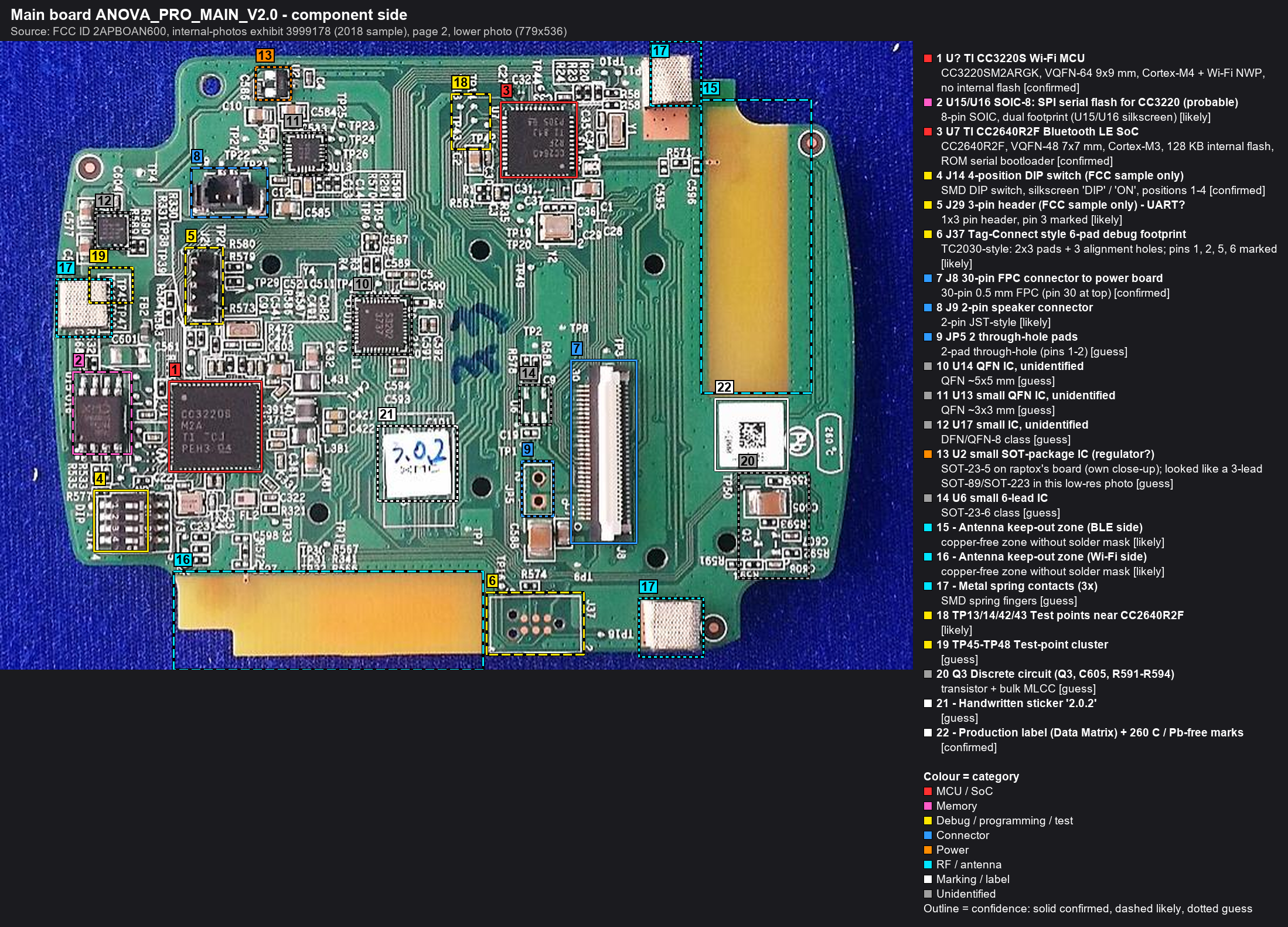
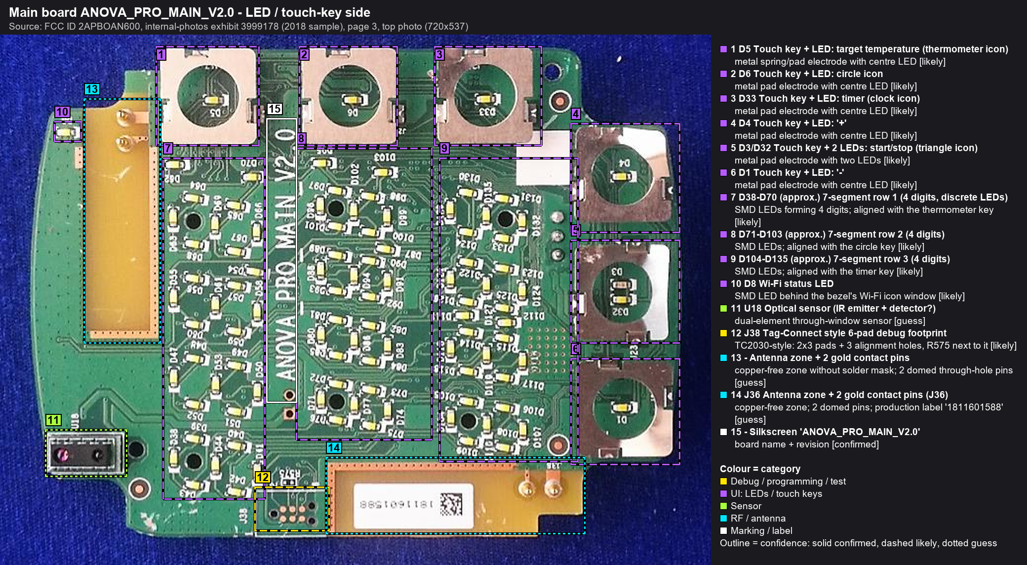
raptox's unit: component side · FCC: component side, LED side | main-board.md |
Power ANOVA_PRO_POWER_REV01 |
FCC: top, bottom | power-board.md |
| Front bezel / light guide | FCC: back view | main-board.md (LED / touch side) |
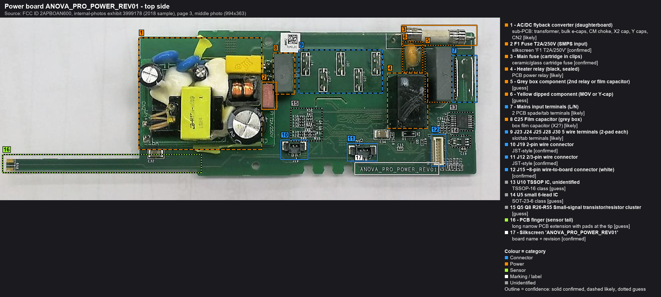
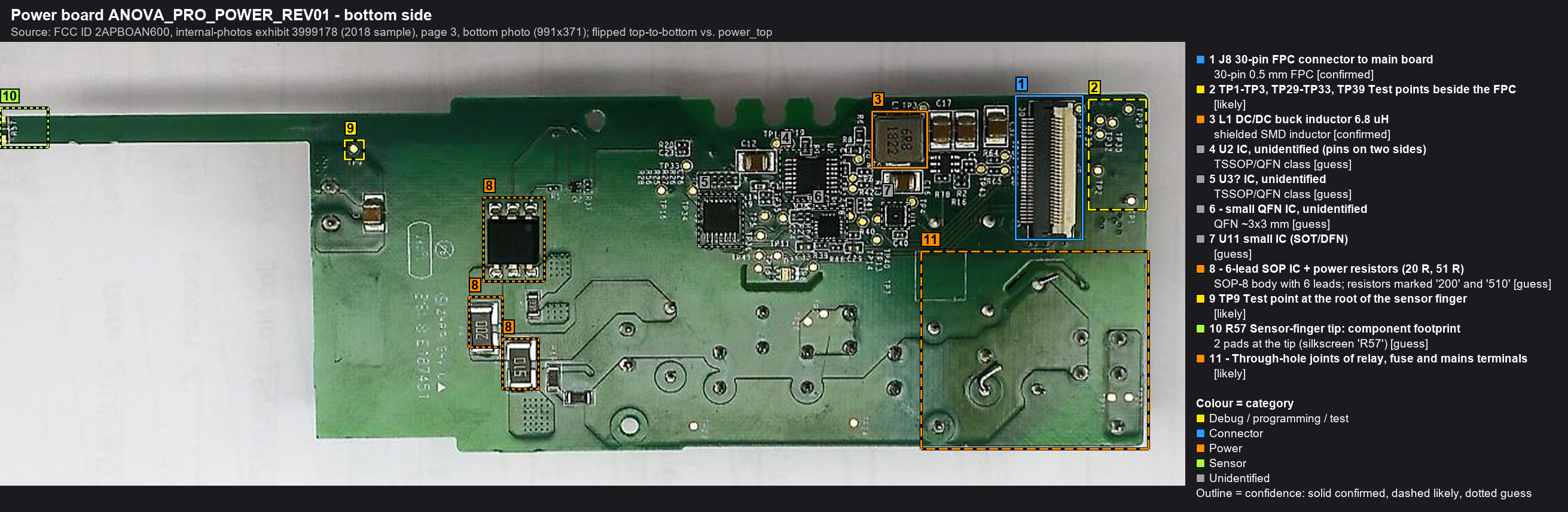
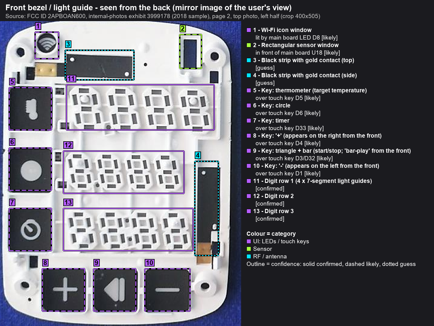
Biggest open questions
- ~~Does raptox's AN600-20 use the same board revisions?~~ Main board: same layout, debug parts not fitted. Power board: not checked yet.
- Which chip(s) did the failed OTA update target: CC3220S app, CC3220 service pack, CC2640R2F, or a power-board MCU?
- Is there an MCU on the power board (U2 is the candidate)?
- What is the pinout of the J8 FFC and the debug footprints (J29, J37, J38), and what do the J14 DIP pads connect to?
- What are U14 (
T3018), U13 (4637) and U17? - Which logic rails exist (3.3 V? 1.8 V?) and are they present on the dead unit?