Main board: ANOVA_PRO_MAIN_V2.0
Two sources: - raptox's unit (AN600-20 EU, opened 2026-11-01): 12 MP photos plus chip close-ups. Callouts: main_component-side_own. - FCC sample (2018 pre-production, low-res). Callouts: component side · LED side.
The layout and reference designators match, so raptox's board is the same PCB design (likely MAIN_V2.0; the silkscreen
name is on the LED side, not yet photographed). The production BOM leaves out the debug parts, see below.
Component side: raptox's unit
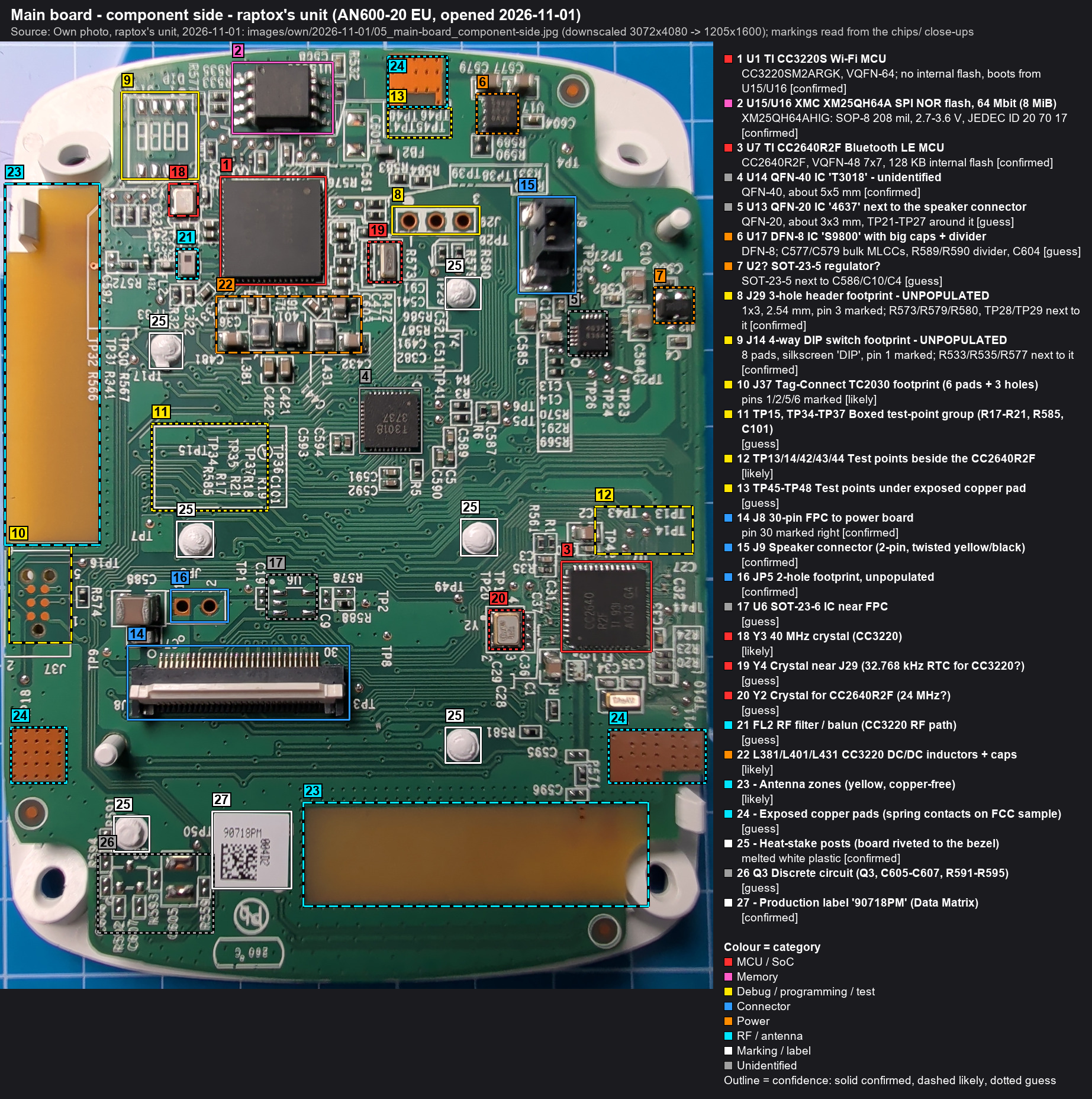
Chip markings (confirmed from close-ups)
| Ref | Marking | Part | Role |
|---|---|---|---|
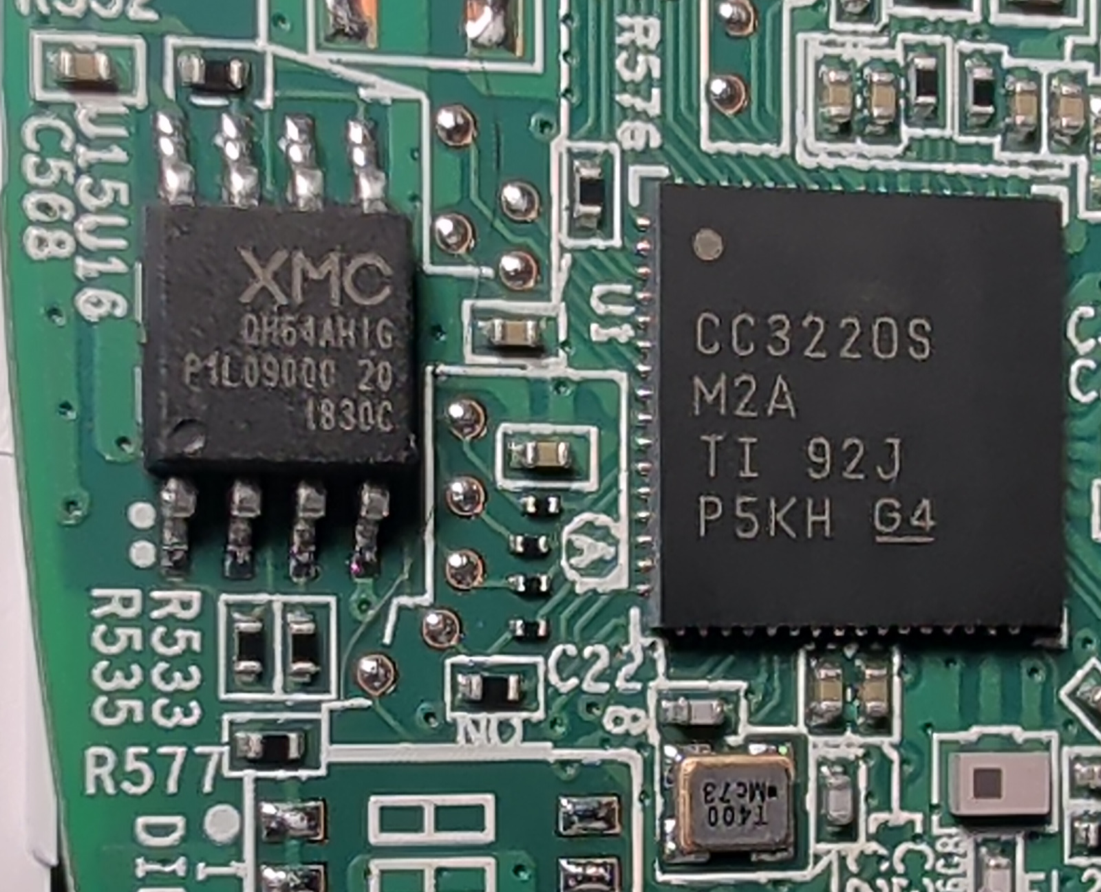
| U1 | CC3220S / M2A / TI 92J / P5KH G4 |
TI CC3220SM2ARGK (VQFN-64) | Wi-Fi MCU. No internal flash, boots from U15/U16. |
| U15/U16 | XMC / QH64AHIG / P1L09000 20 / 1830C |
XMC XM25QH64AHIG: 64 Mbit (8 MiB) SPI NOR, SOP-8 208 mil, 2.7-3.6 V | CC3220 serial flash: firmware + filesystem. Dump target. |
| U7 | CC2640 / R2F / TI 931 / A0J3 G4 |
TI CC2640R2F (VQFN-48 7x7) | BLE MCU, 128 KB internal flash |
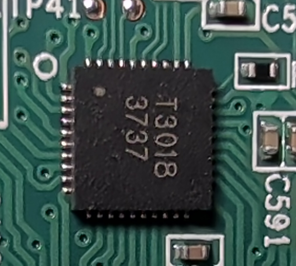
| U14 | T3018 / 3737 |
unidentified QFN-40 (~5x5 mm) | central; LED/touch driver or a third MCU? |
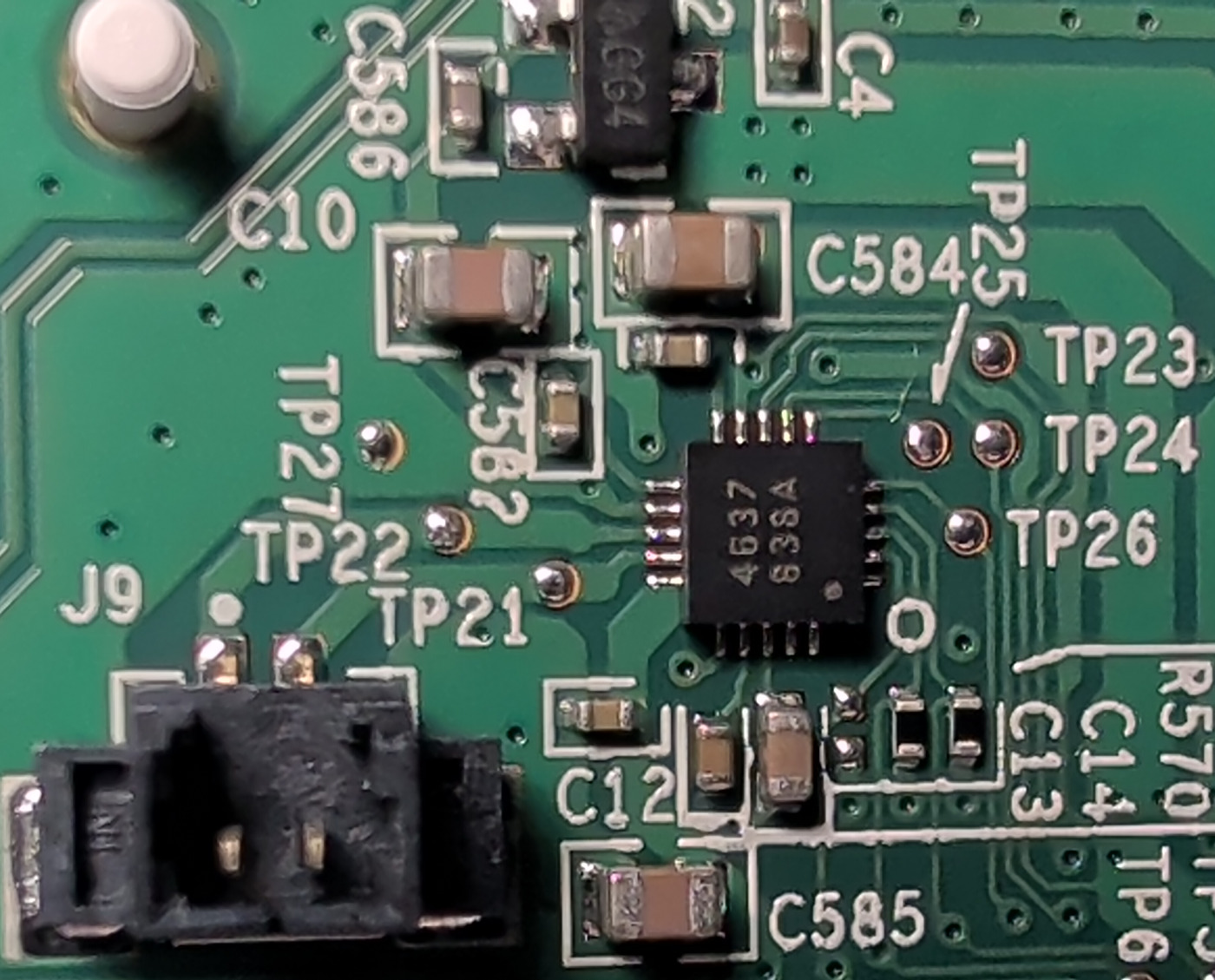
| U13 | 4637 / 638A |
unidentified QFN-20 (~3x3 mm) | right next to the speaker connector J9: audio driver? |
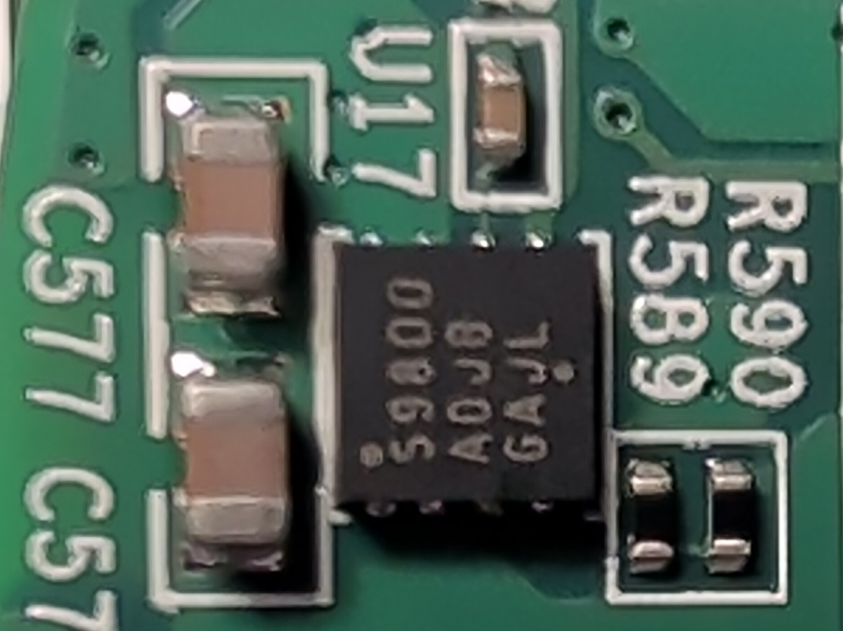
| U17 | S9800 / A0J8 / GAJL (uncertain) |
unidentified DFN-8 | with bulk caps C577/C579 and divider R589/R590: regulator / load switch? |
| U2? | ?CG4 |
SOT-23-5 | regulator? |
| Y3 | T400 / Mc73 |
40 MHz crystal | CC3220 main clock (likely) |
| Y2, Y4, Y1 | - | crystals | CC2640R2F clock, 32 kHz RTC(s) (guess) |
Close-up crops (originals in images/own/2026-11-01/chips/):
 |
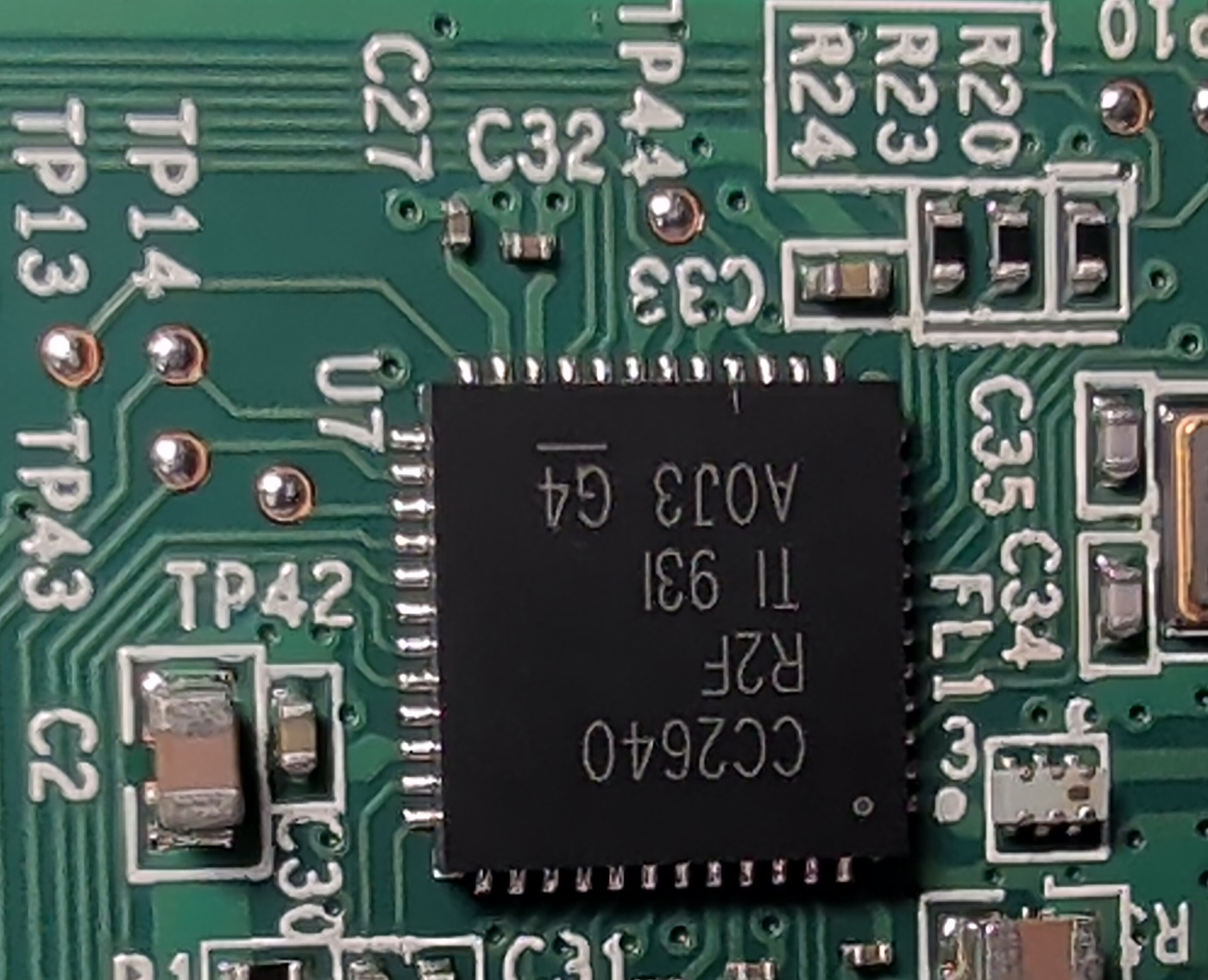 |
| U15/U16 XMC flash, U1 CC3220S, Y3, J14 footprint | U7 CC2640R2F + test points |
 |
 |
U14 T3018 |
U13 4637, TP21-27, J9 speaker, U2 |
 |
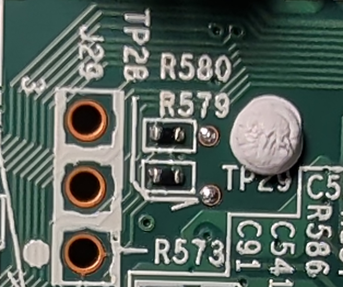 |
| U17 (rotated) | J29 3-hole footprint, TP28/TP29 |
Production unit vs FCC sample
| Item | FCC sample (2018) | raptox's unit | Consequence |
|---|---|---|---|
| J14 DIP switch (4-way) | fitted (orange) | empty footprint | If J14 is confirmed as the SOP straps, a switch or wires on the pads change them |
| J29 header (1x3, 2.54 mm) | fitted | empty holes | Solder a 3-pin header for UART access |
| Spring contacts (3x) | fitted | bare copper pads | probably not needed in production |
| "2.0.2" sticker | yes | no | |
| Chip date codes | flash ?, CC2640 813 |
flash 1830, CC3220 92J, CC2640 931 |
built around 2019 (likely, from the TI date codes) |
Debug / programming candidates
| Ref | What | Hypothesis | How to confirm |
|---|---|---|---|
| J29 | 1x3 holes, pin 3 marked, with TP28/TP29 and R573/R579/R580 | CC3220 UART0 (TX/RX/GND), used by UARTLOAD/Uniflash | continuity to the U1 UART pins; scope at power-up |
| J14 | 4-way DIP footprint near R533/R535/R577 | CC3220 SOP0/1/2 straps (+ nRESET?) | continuity to the U1 SOP pins |
| J37 | Tag-Connect TC2030 (6 pads + 3 holes) | JTAG/SWD (CC3220) or cJTAG (CC2640R2F) | continuity; J38 on the LED side is its twin |
| TP13/14/42/43/44 | test points beside U7 | CC2640R2F cJTAG / reset / UART | continuity to U7 pins |
| TP15, TP34-37 | boxed group with R17-R21, R585, C101 | production test / programming | continuity |
| TP21-27 | around U13 | U13 signals | |
| TP45-48 | under an exposed copper pad | ? |
Connectors
- J8: 30-pin 0.5 mm FPC to the power board (pin 30 at the right in raptox's photo). Pinout TODO.
- J9: 2-pin, speaker (confirmed: twisted yellow/black pair to a round speaker labelled
20 / 219in the housing). - JP5: 2 empty holes. Purpose unknown.
Mechanics
- The board is heat-staked to the white bezel (6 melted posts). Everything needed for Phase 1-3 is on this side, so there is no need to remove it.
- Two yellow antenna zones (left edge, bottom). The CC3220 RF path probably goes via FL2 near U1 (guess).
LED / touch side (FCC sample only so far)
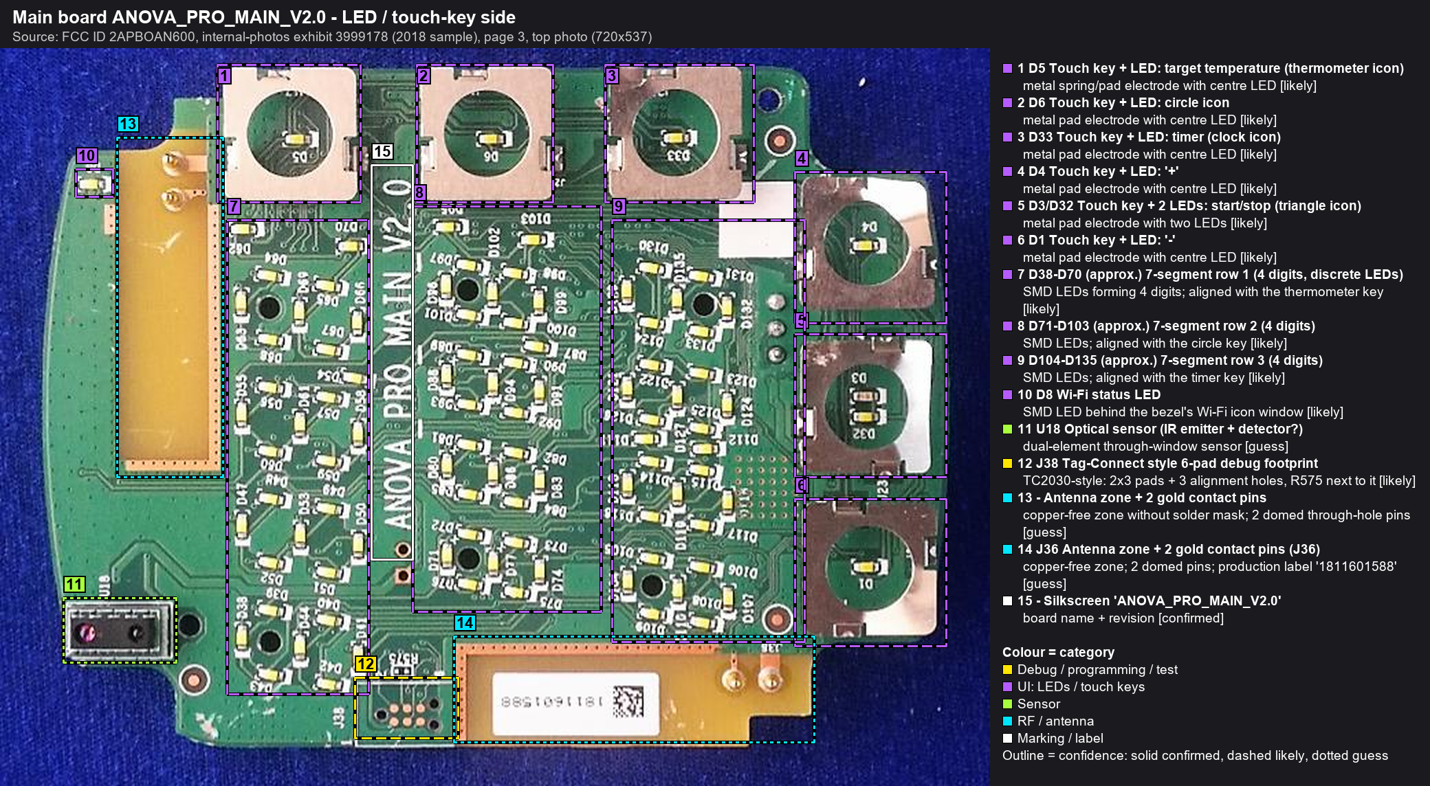
Source: FCC ID 2APBOAN600, internal-photos exhibit 3999178 (2018 sample).
The display is built from discrete SMD LEDs (about D1-D135) behind a white light guide, not an LCD.
The key mapping below comes from overlaying this side on the (mirrored) bezel photo. It is likely:
| Touch key (LED) | Bezel icon | Function (per manual) |
|---|---|---|
| D5 | thermometer | target temperature |
| D6 | filled circle | ? |
| D33 | clock | timer |
| D4 | + | increase |
| D3 + D32 | triangle + bar | start / stop |
| D1 | - | decrease |
- Digit rows (D38-D135 approx.): 3 rows x 4 seven-segment digits.
- D8: Wi-Fi status LED (likely). U18: optical sensor behind the rectangular window (guess).
- J38: Tag-Connect footprint, back-to-back with J37.
- Two copper-free zones with 2 domed gold pins each (one is J36). They contact the two black strips on the bezel (antenna elements? guess).
Open questions
- Map J29, J14 (pads), J37 and the TP groups to U1/U7 pins (continuity, board unpowered).
- Identify U14 (
T3018), U13 (4637), U17 (S9800). Which chip drives the LEDs, touch keys and speaker? - Interconnect between the CC3220S and CC2640R2F (UART? SPI?).
- J8 FPC pinout and rails.
- Confirm the
MAIN_V2.0silkscreen on raptox's board (LED side, not photographed).